Showing posts with label Basic Circuits Explanation. Show all posts

Wednesday, February 13, 2008

Input Offset Voltage Null Circuit

This circuit is application of OP07. adjust variable resistor for null Offset
Voltage output at initrial state


Op07
Op07 represent a breakthrough in operational amplifier performance.
Low offset and long-term stability are achieved by means of a low-noise,

chopperless, bipolar-input-transistor amplifier circuit. For most applications,

external components are not required for offset nulling and
frequency compensation. The true differential input, with a wide input
voltage range and outstanding common-mode rejection, provides
maximum flexibility and performance in high-noise environments and in

noninverting applications. Low bias currents and extremely high input
impedances are maintained over the entire temperature range.
The OP07 is unsurpassed for low-noise, high-accuracy amplification of
very low-level signals.

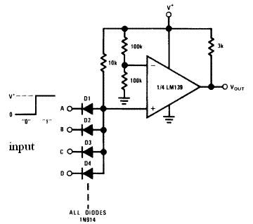
Simple Large Fan-In AND Gate circuit

We can make simple Large Fan-In AND Gate circuit by one Voltage
Comparators from circuit below


Vout = A and B and C and D and ….

This circuit is application of LM139
LM139
Low Power Low Offset Voltage Quad Comparators
The LM139 series consists of four independent precision
voltage comparators with an offset voltage specification as
low as 2 mV max for all four comparators. These were
designed specifically to operate from a single power supply
over a wide range of voltages.

All pins of any unused comparators should be tied to the
negative supply.

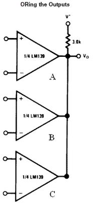
The output of the LM139 series is the uncommitted collector
of a grounded-emitter NPN output transistor. Many collectors
can be tied together to provide an output OR’ing function.


Vo = A or B or C

On-Off Control With Hysteresis Circuit

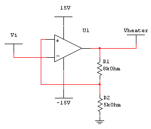
We can use inverting Schmitt trigger circuit for this application
Inverting Schmitt trigger
the circuit can be view as an inverting –type threshold detector whose
threshold is controlled by the out put since the output has two stable
state, this threshold has two possible values,namly


Vth = R1*Voh/(R1+R2)
Vtl = R1*Vol/(R1+R2)


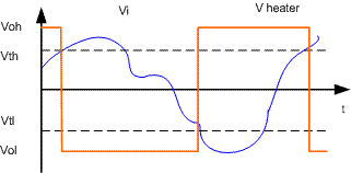
The hysteresis width is defined as
Hw = Vth – Vtl = R1*( Voh – Vol )/( R1 + R2 )

Behaviour of circuit show in below picture.


Sample waveforms

Thermally compensated Zener circuit

Thermal stability is the most demanding performance requirement
Of voltage references

Forward drop of a silicon junction decreases about 2mV for every
degree Celsius increase

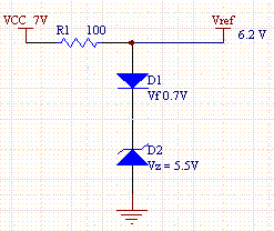
The idea behind thermal compensated Zener diode is to connect a
forward-biased diode in series with a Zener diode having an equal
but opposing thermal voltage (TC)


Vref = Vz+Vf = 5.5+0.7 = 6.2 V
Uses Iz = 7.5 mA
R1 = (Vcc-Vref)/Iz = 106.6 ohm

Ratiometric Linear Hall Effect Sensors

Hall Effect
If an electric current flows through a conductor in a magnetic field,
the magnetic field exerts a transverse force on the moving charge
carriers which tends to push them to one side of the conductor.
This is most evident in a thin flat conductor as illustrated. A buildup
of charge at the sides of the conductors will balance this magnetic
influence, producing a measurable voltage between the two sides of
the conductor. The presence of this measurable transverse voltage
is called the Hall effect
http://230nsc1.phy-astr.gsu.edu/hbase/magnetic/hall.html

The UGN3503LT, UGN3503U, and UGN3503UA Hall-effect
sensors accurately track extremely small changes in magnetic flux
density—changes generally too small to operate Hall-effect switches.


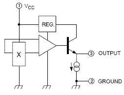
Each Hall-effect integrated circuit includes a Hall sensing element,
linear amplifier, and emitter-follower output stage. Problems associated
with handling tiny analog signals are minimized by having the Hall cell
and amplifier on a single chip.
Application
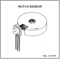
NOTCH SENSOR
The south pole of a magnet is attached to the back of the package if
the Halleffect IC is to sense the presence of ferrous material.

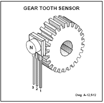
GEAR TOOTH SENSOR
The north pole of a magnet is attached to the back surface if the

integrated circuit is to sense the absence of ferrous matrial.


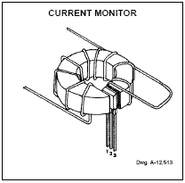
CURRENT MONITOR
proportional output-voltage levels are dependent on magnetic flux
density at the most sensitive area of the device.

Easy 4-bit magnitude comparator circuit

74HC/HCT85 are easy way for 4-bit magnitude comparator circuit

The 74HC/HCT85 are 4-bit magnitude comparators that can be
expanded to almost any length. They perform comparison of
two 4-bit binary, BCD or other monotonic codes and present the
three possible magnitude results at the outputs (QA>B, QA=B and
QA

FUNCTION TABLE

C code for 74165

74165 can use for expender input port of microcontroller
74165 are 8-Bit Parallel In/Serial Output Shift Registerswhich shifts data
in the direction of QA toward QH when clocked.Parallel-in access is made
available by eight individual direct datainputs, which are enabled by a low
level at the shift/loadinput. These registers also feature gated clock inputs
and complementary outputs from the eighth bit.
Timing diagram for read data


C code for control 74165 by microcontroller


74165 to microcontroller circuit

Rotary encoder converter circuit

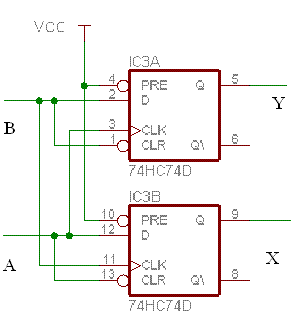
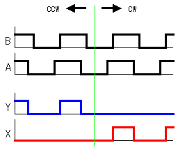
This circuit used convert signal from Rotary encoder (A,B) to two pulse signal
- Y for CCW direction
- X for CW (clockwise) direction
Two pulse signal is easy for microcontroller programing
The circuit used two D-type flip-flop(74HC74D) for the judgement.

Signal input and signal out put

Converter bridge driver signal circuit

Converter PWM and direction to bridge driver signal circuit
This circuit for convert signal PWM (speed) and signal direction from
microcontroller to signal of motor bridge driver circuit. thay is two pwm
signal A for motor turn right and B for motor turn left

4A DC Motor Drive Circuit , Easy PWM generator circuit

PCB Design Paper

Calculation of PCB Track Impedance Paper (PDF)
The use of high-speed circuits requires PCB tracks to be
designed with controlled (characteristic, odd-mode, or
differential) impedances.

Wadell[1] is one of the most comprehensive sources of
equations for evaluating these
impedances.

This source includes many configurations including stripline,
surface microstrip, and their coplanar variants.

Current Carrying Capacity of Vias Paper (PDF)
We are frequently asked about the current carrying
capacity of vias.

To our knowledge, there have been no
studies of this particular topic, although we do know of
people who have useful insights into this issue.

What we offer here are some observations and a conceptual
framework for looking at the issue, with some resulting
guidelines that seem reasonable.


PCB Design Tutorial Paper (PDF)
You've designed your circuit, perhaps even bread boarded
a working prototype, and now it's time to turn it into a nice
Printed Circuit Board (PCB) design. For some designers,
the PCB design will be a natural and easy extension of the
design process. But for many others the process of designing
and laying out a PCB can be a very daunting task.

Isolate 4-20mA to Voltage Circuit

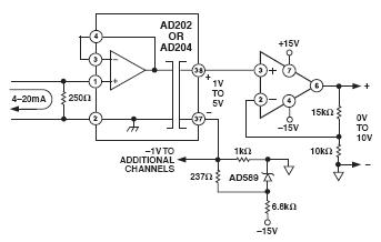
The AD202 and AD204 are general purpose, two-port,
transformer-coupled isolation amplifiers that may be used in
a broad range of applications where input signals must be
measured, processed, and/or transmitted without a galvanic
connection.

AD202/AD204 application circuit

Picture shows an isolator receiver that translates a 4-20 mA
process current signal into a 0 V to 10 V output. A 1 V to 5 V
signal appears at the isolator’s output, and a –1 V reference
applied to output LO provides the necessary level shift
(in multichannel applications, the reference can be shared by
all channels). This technique is often useful for getting offset
with a follower-type output buffer.


The circuit as shown requires a source compliance of at least
5 V
, but if necessary that can be reduced by using a lower value
of current-sampling resistor and configuring the input amplifier
for a small gain.

PCB Clearances Table

For non-mains voltages, the IPC standard has a set of tables
that define the clearance required for various voltages.
A simplified table is shown here. The clearance will vary depending
on whether the tracks are on an internal layers or the external
surface. They also vary with the operational height of the board
above sea level, due to the thinning of the atmosphere at high
altitudes.

PCB Clearances for Electrical Conductors Table
Voltage (DC or Peak AC) - Internal - External (<3050m)

- External (>3050m)
0-15V - 0.05mm - 0.1mm - 0.1mm
16-30V - 0.05mm - 0.1mm - 0.1mm
31-50V - 0.1mm - 0.6mm - 0.6mm
51-100V - 0.1mm - 0.6mm - 1.5mm
101-150V - 0.2mm - 0.6mm - 3.2mm
151-170V - 0.2mm - 1.25mm - 3.2mm
171-250V - 0.2mm - 1.25mm - 6.4mm
251-300V - 0.2mm - 1.25mm - 12.5mm
301-500V - 0.25mm - 2.5mm - 12.5mm

PCB Design Tutorial by David L. Jones

Track Width Reference Table

Track Width Reference Table (for 10deg C temp rise).
Track Width is in Thous (mils)
Current (Amps) - Width for 1oz - Width for 2 oz - milli Ohms/Inch
1 - 10 - 5 - 52
2 - 30 - 15 - 17.2
3 - 50 - 25 - 10.3
4 - 80 - 40 - 6.4
5 - 110 - 55 - 4.7
6 - 150 - 75 - 3.4
7 - 180 - 90 - 2.9
8 - 220 - 110 - 2.3
9 - 260 - 130 - 2.0
10 - 300 - 150 - 1.7


As a start, you may like to use say 25 thou for signal tracks, 50 thou for power
and ground tracks
, and 10-15 thou for going between IC and component pads.
Some designers though like the “look” of smaller signal tracks like 10 or 15 thou,
while others like all of their tracks to be big and “chunky”. Good design practice
is to keep tracks as big as possible, and then to change to a thinner track only
when required to meet clearance requirements.

The thickness of the copper on the PCB is nominally specified in ounces per
square foot, with 1oz copper being the most common. You can order other
thicknesses like 0.5oz, 2oz and 4oz. The thicker copper layers are useful for high
current, high reliability designs.


PCB Design Tutorial by David L. Jones


PCB Track Width Calculator

This page calculates approximations to the
ANSI/IPC-D-275 and IPC-2221 design standards for PCB trace width.
www.desmith.com/NMdS/Electronics/TraceWidth.html

The PCB Track Width Calculator
The PCB Company - Supplier of Printed Circuit Boards.

www.pcbco.com.au/tracecalc.html

PCB Trace Width Calculator
QUESTION: Very cool PCB width tool! I would like to know its limits though.
I entered a 65 amp current requirement and it returned a track width that must

www.geocities.com/capecanaveral/lab/9643/TraceWidth.htm

Voltage to Bar Graph Circuit

if you want to create circuit for display 10-step voltage divider.
This device is easy way for make voltage to bar graph circuit


LM3914 Dot/Bar Display Driver
The LM3914 is a monolithic integrated circuit that senses
analog voltage levels and drives 10 LEDs, providing a linear
analog display. (voltage to bar graph circuit )


Features
- Drives LEDs, LCDs or vacuum fluorescents
- Bar or dot display mode externally selectable
- Expandable to displays of 100 steps
- Internal voltage reference from 1.2V to 12V
- Operates with single supply of less than
- Inputs operate down to ground
- Output current programmable from 2 mA
- No multiplex switching or interaction between
- Input withstands ±35V without damage or
- LED driver outputs are current regulated, open-collectors
- Outputs can interface with TTL or CMOS
- The internal 10-step divider is floating and referenced to a
wide range of voltages

Precision Voltage-to-Current Converter Circuit

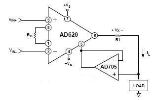
The AD620, along with another op-amp and two resistors, makes
a precision current source circuit.

The op-amp buffers the reference terminal to maintain good CMR.
The output voltage, VX, of the AD620 appears across R1, which
converts it to a current. This current, less only the input bias current
of the op amp, then flows out to the load.
where
Vx = [(Vin+) – (Vin-)] * G
IL = Vx / R1
Circuit operates on 1.8 mA, ±3 V

Gain(G) is resistor-programmed by Rg
Rg = 49.4K ohm / (G-1)

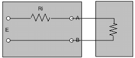
Maximum power of a two terminal device

The input impedance of a two terminal device may be show in
Picture below. The internal resistance Ri were connected in series
With the internal voltage source E. The connecting terminals as A
And B, and the open circuit voltage presented at these terminals is
E


if an external load R in connected to the device , the voltage
Presented at the output terminals will be dependent on the value of
R. The potential presented at the output terminals is


Eab = E*R/(R + Ri)

The power is given by

P = Eab/R =[ [E*R/(R + Ri)]^2] / R

And the maximizing condition

dP/dR = 0

is applied. There results

R = Ri

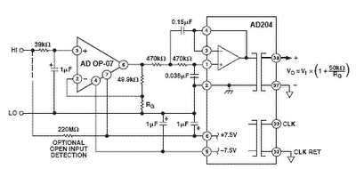
Isolated Thermocouple Transducer Circuit

The AD202 are general purpose, two-port, transformer-
coupled
isolation amplifiers


In applications where the output of thermocouples must be
isolated, a low drift input amplifier can be used with an
AD204,as shown in Picture.

A three-pole active filter is included in the design to
get normal-mode rejection of frequencies above a few Hz
and to provide enhanced common-mode rejection at 60 Hz.
If offset adjustment is needed, it is best done at the trim pins
of the OP07 itself; gain adjustment can be done at the
feedback resistor.
Note that the isolated supply current is large enough to
Mandate the use of 1 mF supply bypass capacitors.

This circuit from AD202 Application

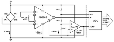
Interfacing Pressure Transducer Circuit

AD620 useful in many bridge applications
the AD620 is especially suitable for higher resistance pressure
Transducer powered at lower voltages where small size and low
Power become more significant.


Picture shows a 3 kΩ pressure transducer bridge powered from 5 V.
In such a circuit, the bridge consumes only 1.7 mA. Adding the
AD620 and a buffered voltage divider allows the signal to be
conditioned for only 3.8 mA of total supply current. Small size and
low cost make the AD620 especially attractive for voltage output
pressure transducers.

Since it delivers low noise and drift, it will also serve applications

such as diagnostic noninvasive blood pressure measurement.

AD620 datasheet pdf

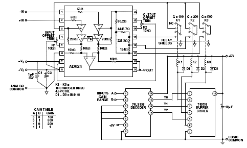
Programmable Gain Thermocouple Amplifier Circuit

AD624 is Instrumentation amplifier of Analog Devices,
designed primarily for use with low level transducers,including
load cells, strain gauges, thermocouple and pressure transducers.


Picture shows the AD624 being used as a software programmable
gain amplifier. Gain switching can be accomplished with
mechanical switches such as DIP switches or reed relays. It
should be noted that the “on” resistance of the switch in series
with the internal gain resistor becomes part of the gain equation
and will have an effect on gain accuracy.


A significant advantage in using the internal gain resistors in a
programmable gain configuration is the minimization of thermocouple
signals which are often present in multiplexed data
acquisition systems.
If the full performance of the AD624 is to be achieved, the user
must be extremely careful in designing and laying out his circuit
to minimize the remaining thermocouple signals.

Selecting a Transducer

Selection of the appropriate transducer is therefore the first and most
importance step in obtaining accurate results. The equations should be
asked before a transducer can be select
- What is the physical quantity to be measured ?
For determining the type and range of the measureand.
- Which transducer principle can best be used to measure this quantity?
For determining the input and output characteristic of the
transducer be compatible with the recording or measurement system.
- What accuracy is required for this measurement?
The accuracy requirement of the total system determine the
degree to which individual factor contributing to accuracy must be
considered. Some of these factors are
1. basic electronic and mechanical characteristic of the transducer
- Type and range of measurand
- Sensitivity
- Excitation
- Mechanical and electrical connection
- Mounting provisions
- Corrosion resistance
2. Transducer accuracy , as an independent component
- Nonlinearity effect
- Hysteresis effect
- Frequency response
- Resolution
3. Transducer’s compatibility
- Zero balance provisions
- Sensitivity tolerance
- Impedance matching
- Insulation resistance

Archive